GaN Foundry Landscape Shifts: TSMC Exits, Infineon Advances
As one of the third-generation semiconductor materials, gallium nitride (GaN) is accelerating its penetration into high-growth areas such as power electronics, data centers, and new energy vehicles, thanks to its high electron mobility, large breakdown voltage, and fast frequency response. However, at this critical juncture, TSMC and Infineon have chosen completely different development paths.
1. TSMC's Exit
TSMC plans to gradually exit the GaN wafer foundry business by 2027. The main reasons include low capacity utilization, intense price competition, and a strategic shift in focus. TSMC's GaN business has primarily focused on 150 mm (6-inch) silicon substrate processes, serving customers such as Navitas, STMicroelectronics, and GaN Systems with high-voltage GaN wafer manufacturing foundry services. However, the overall GaN market is much smaller than that of CMOS, making it difficult to achieve economies of scale in pricing. As a result, TSMC's GaN business has always maintained a low wafer input scale.
From a technical perspective, GaN epitaxial growth has extremely high requirements for temperature control and defect density, posing challenges to equipment and process parameter windows. Additionally, while GaN-on-Si has cost advantages, the mismatch in lattice constants and thermal expansion coefficients makes wafer stress management a key issue. Although TSMC has partially addressed these issues through deposition techniques and stress-relief structures, it still struggles to match silicon devices in terms of process generalization and yield control.
2. Infineon's Advancement
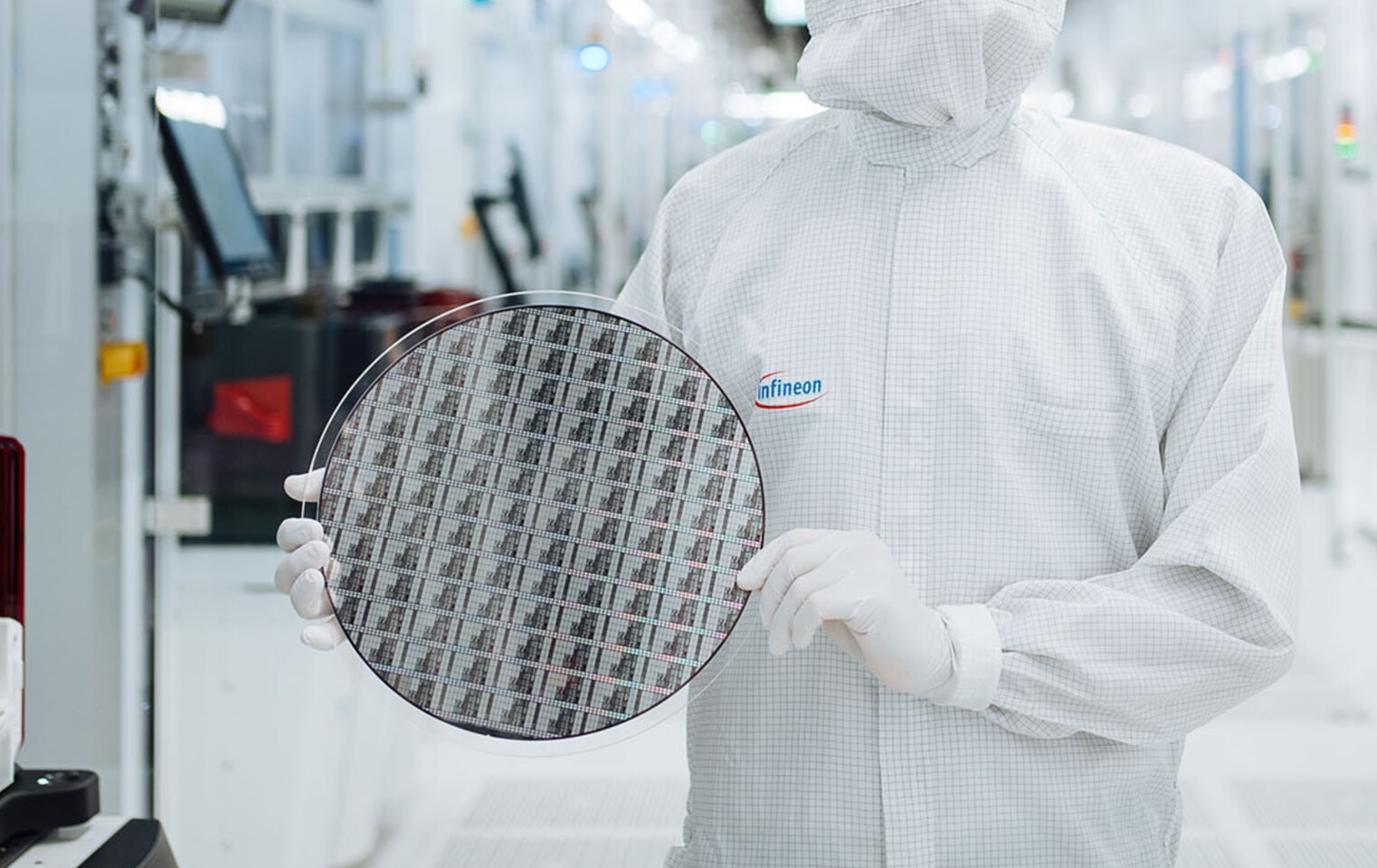
 Meanwhile, Infineon is aggressively advancing its 300 mm GaN wafer IDM (Integrated Device Manufacturing) in-house production line, aiming to gain a first-mover advantage in efficiency and cost. Infineon's strategy is to build an IDM vertical integration model and directly transition to a 300 mm wafer platform. Technically, the biggest advantage of a 300 mm wafer is the significant increase in the number of chips per wafer. According to Infineon's estimates, under the same conditions, each wafer can produce approximately 2.7 times more chips, thereby significantly reducing epitaxial costs and front-end process expenses. A larger wafer platform can also further improve the utilization rate of epitaxial equipment, reduce manufacturing costs, and facilitate standardized testing processes. This is crucial for the future penetration of GaN into high-volume application areas such as automotive and industrial inverters.
Infineon's 300 mm GaN pilot production line aims to start sampling in the fourth quarter of 2025, initially targeting 48V AI power supplies and electric vehicle fast-charging applications.
Engineering Challenges and Supply Chain Upheaval in Industry Transition
TSMC's gradual exit has triggered a shift in orders from its major customer, Navitas. Navitas is a typical "fabless GaN" company, with products covering a range from 100V to 650V, widely used in fast charging, power electronics, and AI data centers. Currently, the company has partnered with Power Integrations to transfer its GaN foundry business to the latter's 8-inch production line and build GaN-on-Si manufacturing capabilities based on a 0.18-micron CMOS process platform. However, GaN epitaxial growth technology is significantly different from CMOS, with key challenges including low defect density control, uniformity of epitaxial layer thickness, and stress-relief mechanisms. Additionally, the testing process for GaN wafers requires specialized platforms due to their high-voltage characteristics and breakdown capabilities, posing higher demands on the engineering capabilities of wafer fabs. TSMC faces validation pressure to achieve equivalent reliability and output scale in the short term.
From a supply chain perspective, TSMC's exit has created opportunities for China and other emerging GaN manufacturers. Several domestic IDMs and foundries, including CRMicro, Unisoc, and Hua Hong Grace, have announced the completion of GaN production lines, which are competitive in terms of cost, delivery time, and regional service. However, the stable supply of high-quality epitaxial wafers remains a limiting factor. GaN epitaxial vendors such as Veeco (US), Yu Jing (Taiwan), and Aixtron (Europe) hold key equipment and process know-how, with some core equipment not yet fully localized. In the future, packaging standards and forms (such as DFN, FC) will also affect the promotion of GaN at the system level.
Future Outlook
TSMC's retreat and Infineon's push represent two typical industry paths: the former chooses to avoid non-core resource consumption, while the latter focuses on high vertical integration and large wafer technology. As the GaN market continues to develop, the future GaN foundry landscape will become more diversified. On one hand, the advantages of the IDM model in cost control and technological innovation will gradually emerge; on the other hand, the foundry model will still play an important role in specific areas. Whether it is IDM or foundry, the development of the GaN industry requires comprehensive consideration in terms of technology, cost, and supply chain to achieve sustainable development.
Conevo Integrated Circuits Supplier
Conevo is a leading distributor of IC chips, renowned for its extensive ic product and reliable service. We specialize in providing high-performance IC parts to meet diverse market needs. Here are some of our popular and carefully selected chip models:
● XC3S1600E-4FGG400I: A high-density FPGA with extensive logic resources, ideal for complex digital designs.
● TPS22917DBVR: A robust power switch, designed for efficient power management and protection in various applications.
● BCM5464RA1KFBG: A high-speed Ethernet transceiver, offering reliable data transmission for networking solutions.
Website: www.conevoelec.com
Email: info@conevoelec.com


