Sony's New Generation of Image Sensors for Smartphones
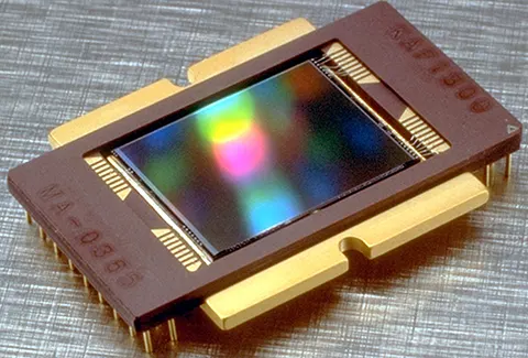
 Sony Semiconductor Solutions, a subsidiary of Sony Group, is set to supply next-generation image sensors to smartphones by March 2030. The new CMOS (complementary metal-oxide-semiconductor) sensors will feature a 3-layer structure, compared to the previous 2-layer design. The semiconductor's circuit linewidth will be reduced from 40 nanometers to 22-28 nanometers, with customization for image sensors. This advancement enables improvements in sensitivity, resolution, and read-out speed without altering the sensor's size.
The new CMOS sensors will undergo a significant upgrade in architecture. The current dual-layer design of Sony's stacked CMOS sensors, which includes a photodiode layer for light-sensing pixels and a logic circuit layer for image processing, will be enhanced with a third processing layer. This additional layer will significantly expand the sensor's image-processing capabilities. The adoption of 22-28-nanometer process technology, specifically tailored for image sensors, will further enhance performance.
New Image Sensors Performance Enhancements
The transition to a 3-layer structure and the new process technology will result in comprehensive performance improvements. The new sensors are expected to achieve higher sensitivity, resolution, and read-out speed. Faster read-out speeds will positively impact various aspects of camera performance, such as reducing the rolling shutter effect, increasing burst-shooting speed, and enhancing autofocus performance. Additionally, Sony's latest sensor technology has achieved a breakthrough in dynamic range, with the recently unveiled IMX09E sensor supporting Hybrid Frame-HDR technology and a dynamic range exceeding 100dB.
Market Strategy and Future Prospects
Sony aims to maintain its leading position in the global CMOS image sensor market. Despite facing competition from Samsung Electronics and the potential for Apple to source sensors from other suppliers, Sony is confident about its future prospects. The company's president, Teruhiko Mine, has stated that commercial negotiations for the new sensors are largely completed, and the focus is on the period after 2030. Sony plans to achieve a 60% global market share for CMOS image sensors by 2025.
Sony's investment in new sensor technologies, including multi-layer stacked CMOS sensors, demonstrates its commitment to innovation and maintaining a competitive edge. The company's long-term goal is to enhance sensor-level processing capabilities, which will improve dynamic range, sensitivity, noise performance, efficiency, read-out speed, and resolution. This focus on advanced sensor technologies will not only benefit Sony's camera products but also strengthen its position in the smartphone market.
Conevo semiconductor chip distributor
Conevo is a global semiconductor chip distributor, dedicated to providing customers with high-performance and highly reliable integrated circuit (IC) solutions. Conevo offers a wide range of IC products, including but not limited to analog switches, power management chips, FPGA chips, etc. The rich chip inventory can meet the needs of different customers and ensure rapid delivery. The following are the IC models selected and recommended by Conevo:
● PCF7952ATT/M1CC15118: A high-performance analog switch suitable for signal switching in a variety of electronic devices.
● TPS74518PQWDRVRQ1: An efficient power management chip specifically designed for automotive electronic applications, ensuring stable and reliable power supply.
● XCKU085-2FLVA1517I: An advanced FPGA chip, suitable for complex data processing and high-speed communication systems.
Website: www.conevoelec.com
Email: info@conevoelec.com


