


74AUP1G97GW,125
| Parameters | |
|---|---|
| Series | 74AUP |
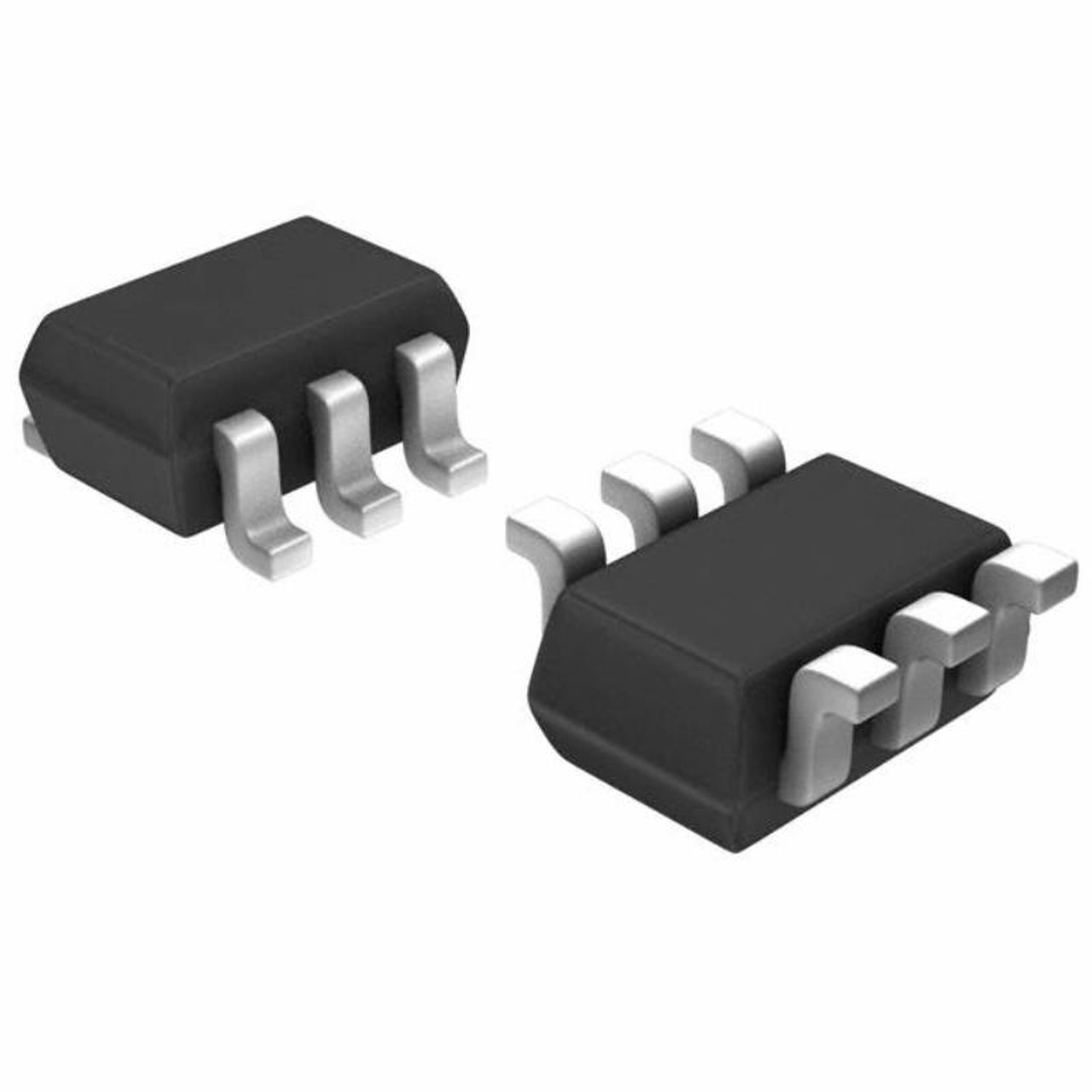
| Package / Case | 6-TSSOP, SC-88, SOT-363 |
| Mfr | NXP USA Inc. |
| Mounting Type | Surface Mount |
| Operating Temperature | -40°C ~ 125°C |
| Output Type | Single-Ended |
| Number of Circuits | 1 |
| Supplier Device Package | SOT-363 |
| Number of Inputs | 3 |
| Voltage - Supply | 0.8V ~ 3.6V |
| Schmitt Trigger Input | Yes |
| Current - Output High, Low | 4mA, 4mA |
| Logic Type | Configurable Multiple Function |
| Package | Bulk |
| Product Status | Active |
| Base Product Number | 74AUP1G97 |
| Standard Package | 1 |
| ECCN | EAR99 |
| HTSUS | 8542.39.0001 |
74AUP1G97GW,125 Configurable Multiple 1 Circuit 3 Input
The 74AUP1G97GW,125 from Nexperia is an advanced low-power configurable multiple-function gate designed for ultra-low voltage applications requiring flexible logic functionality in space-constrained designs. This innovative single-gate IC implements the Boolean function Y = A + B·C in a compact 6-pin SOT353 package, operating from a wide voltage range of 0.8V to 3.6V with a typical static current consumption of just 0.9 μA, making it ideal for battery-powered portable electronics, IoT devices, and mobile applications where power efficiency and board space optimization are critical. The device features a configurable logic architecture that can be programmed through input pin connections to function as a two-input AND gate followed by a two-input OR gate, providing designers with versatile logic implementation capabilities without requiring multiple discrete components. With its CMOS technology offering high noise immunity and balanced propagation delays typically under 4.2 ns at 3.3V, the 74AUP1G97GW,125 enables reliable signal processing in applications such as power management sequencing, signal gating, and interface logic conditioning while maintaining exceptional power efficiency.
74AUP1G97GW,125 Gate IC Applications
The 74AUP1G97GW,125 is extensively used in smartphones and tablets for power sequencing circuits, enabling controlled power-up/power-down sequences for various subsystems while minimizing component count and power consumption. IoT sensor nodes and wearable devices utilize this configurable gate for signal conditioning, wake-up logic, and power management functions where its ultra-low power characteristics extend battery life. Industrial automation systems employ the device for interface logic between sensors and microcontrollers, implementing simple state machines and control logic in PLCs and sensor interfaces. Consumer electronics applications include portable media players, digital cameras, and gaming accessories where space constraints and power efficiency are paramount. Additional applications include medical monitoring devices, automotive electronics, and communication equipment that benefit from the device's reliability, wide voltage range, and temperature tolerance in demanding operating environments.
Alternative Configurable Logic Gate Recommendations
● SN74LVC1G97DBVR (Texas Instruments): A single configurable multiple-function gate with similar functionality operating from 1.65V to 5.5V supply range in a SOT23-6 package.
● MC74VHC1G97DFT2G (ON Semiconductor): A high-speed CMOS configurable logic gate featuring 2.0V to 5.5V operation with 10.5 ns propagation delay at 5V.
● NC7SZ97L6X (Fairchild/ON Semiconductor): An ultra-low power configurable multiple-function gate with 1.65V to 5.5V operation in a SC-70 package.
● TC7SZ97FU(TE85L,F) (Toshiba): A single configurable logic gate operating from 1.65V to 5.5V with 4.8 ns typical propagation delay at 3.3V.


