From 8 to 12 Inch: NXP's Strategic Shift in Wafer Production
NXP, a global leader in the semiconductor industry, has recently announced a significant strategic adjustment plan. Over the next decade, the company will gradually close four 8-inch wafer fabs and shift its production focus entirely to 12-inch wafer fabs. Among the four 8-inch fabs planned for closure, one is located in Nijmegen, the Netherlands, while the other three are in the United States.
 This decision is driven by the industry-wide trend of migrating from 8-inch to 12-inch wafer manufacturing technology. Compared to 8-inch wafers, 12-inch wafers can produce 2.25 times the number of chips per wafer, assuming no edge loss. This means that under the same process conditions, 12-inch wafers can significantly reduce fixed costs and unit manufacturing costs, thereby enhancing the company's profitability and market competitiveness. Moreover, with the rapid development of emerging technologies such as artificial intelligence, data centers, and autonomous driving, the market demand for high-performance and highly integrated chips is continuously increasing. The higher production efficiency and more advanced linewidth precision of 12-inch wafers give them a greater advantage in meeting these high-end application requirements.
Construction and Significance of the 12-Inch Fab in Singapore
To smoothly transition from 8-inch to 12-inch wafer manufacturing, NXP has established a joint venture with VIS in Singapore, forming the VSMC company. The company plans to invest $7.8 billion to build a 12-inch wafer fab. The new facility is expected to begin mass production in 2027, focusing on the production of mixed-signal, power management, and analog chips with process nodes ranging from 130nm to 40nm. By 2029, the monthly production capacity of this fab is projected to reach 55,000 wafers, making Singapore a key manufacturing hub for NXP in the Asia-Pacific region.
Through this joint venture, NXP can share the high capital expenditure and R&D risks associated with the construction of a new 12-inch fab. Additionally, by leveraging the advanced technology and experience of VIS, NXP can accelerate the construction and operation of the new facility. This cooperation model provides a stronger foundation for NXP's global semiconductor industry layout and enhances its regional coverage in the global supply chain.
The Role and Future of the Nijmegen Site
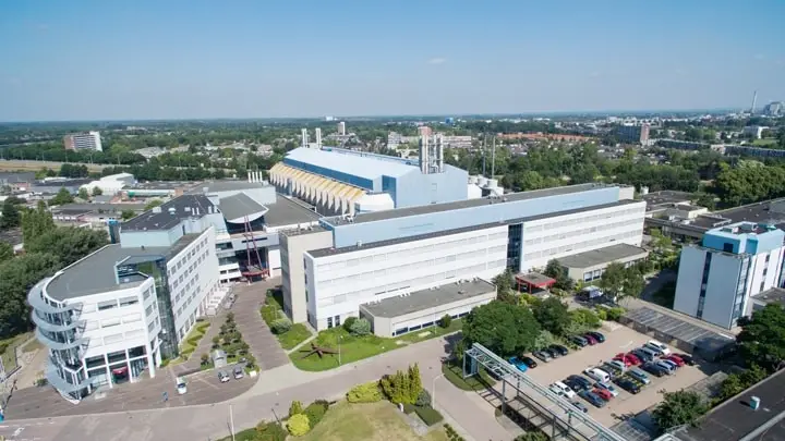
Nijmegen is a crucial base for NXP in the Netherlands, responsible not only for manufacturing but also for key functions such as R&D, testing, technology enablement, and support. The Nijmegen facility plays a vital role in the introduction of new products. Despite the strategic adjustment involving the closure of the 8-inch fab in Nijmegen, NXP has stated that it will continue to maintain its key functions at this site to ensure a smooth business transition.
Moreover, the strategic importance of the Nijmegen base has not been diminished by the closure of the 8-inch fab. On the contrary, with the introduction of 12-inch wafer technology, Nijmegen is expected to play an even greater role in R&D and technological innovation. By optimizing resource allocation, NXP can better focus on high-value-added technology R&D and product innovation in Nijmegen, further consolidating its leading position in the global semiconductor market.
Industry Trends and NXP's Strategic Alignment
NXP's strategic transformation is a microcosm of the global semiconductor industry's upgrade. With continuous technological advancements, 12-inch wafers now account for approximately 65% of the total semiconductor wafer shipments, while the market share of 8-inch wafers is gradually being squeezed. According to data from SEMI, between 2023 and 2026, the global industry is expected to build 82 new 12-inch chip facilities and production lines. By 2026, the monthly production capacity of 12-inch fabs is projected to reach 9.6 million wafers.
In this context, NXP's transformation not only aligns with the overall industry trend but also gains a head start in the future market by making early strategic moves. By closing 8-inch fabs and shifting to 12-inch manufacturing, NXP can better cope with the waves of technological iteration in the semiconductor industry and enhance its competitiveness in the global market.
Conevo IC: Semiconductor Distributor
Looking for reliable semiconductor chips? Conevo IC is your go-to distributor. We specialize in providing high-quality, innovative ic solutions to meet your diverse needs. Here are a few of our top recommended IC models:
● ISL95808HRZ-T: A high-efficiency power management IC, ideal for battery-powered devices.
● EP4CE22E22I7: A versatile FPGA, perfect for embedded systems and IoT applications.
● TPS51200DRCR: A high-performance DC-DC converter, designed for high-current applications.
Website: www.conevoelec.com
Email: info@conevoelec.com


